- 您现在的位置:买卖IC网 > Sheet目录2003 > LTC1278-4IN#PBF (Linear Technology)IC A/DCONV SAMPLNG W/SHTDN 24DIP
15
LTC1278
U
S
A
O
PPLICATI
WU
U
I FOR ATIO
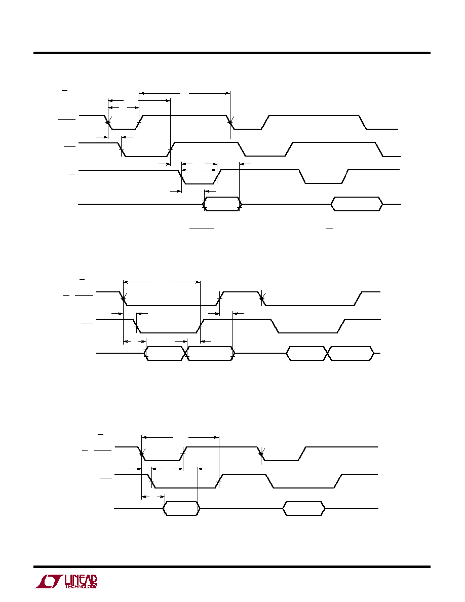
Figure 14. Mode 2. CONVST Starts a Conversion. Data is Read by RD
Figure 15. Slow Memory Mode
Figure 16. ROM Mode Timing
RD = CONVST
BUSY
LTC1278 F15
CS = 0
tCONV
t5
DATA (N – 1)
DB11 TO DB0
DATA
DATA N
DB11 TO DB0
DATA (N + 1)
DB11-DB0
DATA N
DB11 TO DB0
t9
t8
t6
SAMPLE N
SAMPLE N + 1
RD = CONVST
BUSY
LTC1278 F16
CS = 0
tCONV
t5
DATA (N – 1)
DB11 TO DB0
DATA
DATA N
DB11 TO DB0
t8
t9
SAMPLE N
SAMPLE N + 1
CONVST
BUSY
LTC1278 F14
t4
tCONV
CS = 0
t11
t5
t7
t10
DATA N
DB11 TO DB0
DATA (N + 1)
DB11 TO DB0
t9
t8
RD
DATA
SAMPLE N
SAMPLE N + 1
Information furnished by Linear Technology Corporation is believed to be accurate and reliable.
However, no responsibility is assumed for its use. Linear Technology Corporation makes no represen-
tation that the interconnection of its circuits as described herein will not infringe on existing patent rights.
发布紧急采购,3分钟左右您将得到回复。
相关PDF资料
LTC1279CG#TRPBF
IC A/DCONV SAMPLNG W/SHTDN24SSOP
LTC1282ACN#PBF
IC A/D CONV SAMPLING W/REF 24DIP
LTC1288IS8#TRPBF
IC A/D CONV SAMPLING 12BIT 8SOIC
LTC1298IS8#TRPBF
IC A/D CONV SAMPLING 12BIT 8SOIC
LTC1327CNW#PBF
IC TXRX EIA/TIA-562 3.3V 28-DIP
LTC1329ACS8-50#TRPBF
IC D/A CONV 8BIT MICROPWR 8-SOIC
LTC1337CNW#PBF
IC 3DVR/5RCVR 5V RS232 28-DIP
LTC1382IN#PBF
IC TXRX 5V RS232 W/SHTDWN 18-DIP
相关代理商/技术参数
LTC1278-4ISW
功能描述:IC A/DCONV SAMPLNG W/SHTDN24SOIC RoHS:否 类别:集成电路 (IC) >> 数据采集 - 模数转换器 系列:- 标准包装:1,000 系列:- 位数:12 采样率(每秒):300k 数据接口:并联 转换器数目:1 功率耗散(最大):75mW 电压电源:单电源 工作温度:0°C ~ 70°C 安装类型:表面贴装 封装/外壳:24-SOIC(0.295",7.50mm 宽) 供应商设备封装:24-SOIC 包装:带卷 (TR) 输入数目和类型:1 个单端,单极;1 个单端,双极
LTC1278-4ISW#PBF
功能描述:IC A/DCONV SAMPLNG W/SHTDN24SOIC RoHS:是 类别:集成电路 (IC) >> 数据采集 - 模数转换器 系列:- 标准包装:1,000 系列:- 位数:12 采样率(每秒):300k 数据接口:并联 转换器数目:1 功率耗散(最大):75mW 电压电源:单电源 工作温度:0°C ~ 70°C 安装类型:表面贴装 封装/外壳:24-SOIC(0.295",7.50mm 宽) 供应商设备封装:24-SOIC 包装:带卷 (TR) 输入数目和类型:1 个单端,单极;1 个单端,双极
LTC1278-4ISW#TR
功能描述:IC ADC 12BIT SAMPL SHTDWN 24SOIC RoHS:否 类别:集成电路 (IC) >> 数据采集 - 模数转换器 系列:- 标准包装:1,000 系列:- 位数:12 采样率(每秒):300k 数据接口:并联 转换器数目:1 功率耗散(最大):75mW 电压电源:单电源 工作温度:0°C ~ 70°C 安装类型:表面贴装 封装/外壳:24-SOIC(0.295",7.50mm 宽) 供应商设备封装:24-SOIC 包装:带卷 (TR) 输入数目和类型:1 个单端,单极;1 个单端,双极
LTC1278-4ISW#TRPBF
功能描述:IC A/DCONV SAMPLNG W/SHTDN24SOIC RoHS:是 类别:集成电路 (IC) >> 数据采集 - 模数转换器 系列:- 标准包装:1,000 系列:- 位数:12 采样率(每秒):300k 数据接口:并联 转换器数目:1 功率耗散(最大):75mW 电压电源:单电源 工作温度:0°C ~ 70°C 安装类型:表面贴装 封装/外壳:24-SOIC(0.295",7.50mm 宽) 供应商设备封装:24-SOIC 包装:带卷 (TR) 输入数目和类型:1 个单端,单极;1 个单端,双极
LTC1278-5CSW
功能描述:IC A/DCONV SAMPLNG W/SHTDN24SOIC RoHS:否 类别:集成电路 (IC) >> 数据采集 - 模数转换器 系列:- 其它有关文件:TSA1204 View All Specifications 标准包装:1 系列:- 位数:12 采样率(每秒):20M 数据接口:并联 转换器数目:2 功率耗散(最大):155mW 电压电源:模拟和数字 工作温度:-40°C ~ 85°C 安装类型:表面贴装 封装/外壳:48-TQFP 供应商设备封装:48-TQFP(7x7) 包装:Digi-Reel® 输入数目和类型:4 个单端,单极;2 个差分,单极 产品目录页面:1156 (CN2011-ZH PDF) 其它名称:497-5435-6
LTC1278-5CSW#PBF
功能描述:IC A/DCONV SAMPLNG W/SHTDN24SOIC RoHS:是 类别:集成电路 (IC) >> 数据采集 - 模数转换器 系列:- 其它有关文件:TSA1204 View All Specifications 标准包装:1 系列:- 位数:12 采样率(每秒):20M 数据接口:并联 转换器数目:2 功率耗散(最大):155mW 电压电源:模拟和数字 工作温度:-40°C ~ 85°C 安装类型:表面贴装 封装/外壳:48-TQFP 供应商设备封装:48-TQFP(7x7) 包装:Digi-Reel® 输入数目和类型:4 个单端,单极;2 个差分,单极 产品目录页面:1156 (CN2011-ZH PDF) 其它名称:497-5435-6
LTC1278-5CSW#TR
功能描述:IC ADC 12BIT SAMPL SHTDWN 24SOIC RoHS:否 类别:集成电路 (IC) >> 数据采集 - 模数转换器 系列:- 标准包装:1,000 系列:- 位数:12 采样率(每秒):300k 数据接口:并联 转换器数目:1 功率耗散(最大):75mW 电压电源:单电源 工作温度:0°C ~ 70°C 安装类型:表面贴装 封装/外壳:24-SOIC(0.295",7.50mm 宽) 供应商设备封装:24-SOIC 包装:带卷 (TR) 输入数目和类型:1 个单端,单极;1 个单端,双极
LTC1278-5CSW#TRPBF
功能描述:IC A/DCONV SAMPLNG W/SHTDN24SOIC RoHS:是 类别:集成电路 (IC) >> 数据采集 - 模数转换器 系列:- 标准包装:1,000 系列:- 位数:12 采样率(每秒):300k 数据接口:并联 转换器数目:1 功率耗散(最大):75mW 电压电源:单电源 工作温度:0°C ~ 70°C 安装类型:表面贴装 封装/外壳:24-SOIC(0.295",7.50mm 宽) 供应商设备封装:24-SOIC 包装:带卷 (TR) 输入数目和类型:1 个单端,单极;1 个单端,双极